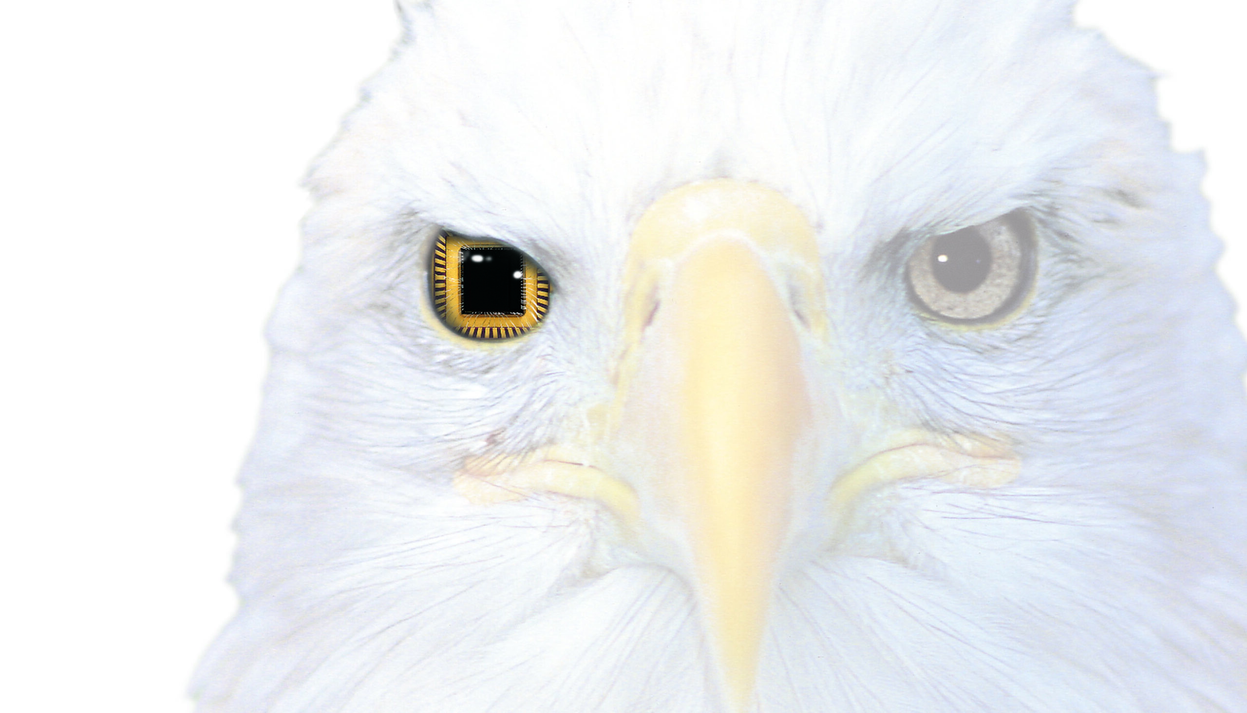
SUNNYVALE, Calif. — February 5, 2001 — OMNIVISION Technologies, Inc. (Nasdaq: OVTI), a leader in designing, developing and marketing advanced, single-chip CMOS image sensors used in electronic cameras and other optical imaging devices, today announced it has shipped its 10 millionth single-chip CMOS image sensor. OMNIVISION offers a full line of single-ship CMOS image sensors, covering the spectrum of CIF (320 x 240) and VGA (640 x 480) pixel resolutions, digital and analog (NTSC and PAL) output, multiple lens size formats, 3.3 to 5.0 volts and either color or black and white imagery.
Founded in 1995, OMNIVISION Technologies supplies the most highly integrated single-chip image sensor, as the Company is able to integrate nearly all camera functions into a single chip. The company invented and patented the technology enabling this high degree of integration. OMNIVISION holds and has applied for 53 patents, creating a significant barrier to entry for other companies trying to enter this market.
OMNIVISION, a fabless semiconductor company, has forged informal strategic relationships with world-class contract manufacturers that have the capacity to meet large volume requirements. “Our customers are not only looking for high quality, small size, low-power consumption and low cost, but they need a supplier that can meet volume requirements,” said Hank O’Hara, vice president of worldwide sales for OMNIVISION Technologies. “OMNIVISION’s past performance has shown that it has the production technology and capacity to deliver quality image sensors at high volumes.”
As optical devices, image sensors are highly sensitive to even a microscopic particle of dust. OMNIVISION performs the final testing on all of its products at its facility in Sunnyvale, California to ensure the quality of every image sensor shipped. OMNIVISION designed and built its own automatic testing equipment which actually fires-up the chip and does a computer analysis of the resulting image. Final testing can be a significant barrier to entry for large-scale production, and OMNIVISION has a sophisticated solution that enables it to quickly ramp-up production.
“OMNIVISION owes much of its success to its extensive research and development program,” continued Mr. O’Hara. “Our R&D; programs are focused on creating smaller die, designing for lower voltage and providing higher resolutions, including SVGA (800 x 600) and mega-pixel (1280 x 1024) products. We are aggressively attempting to add new image sensors to the twelve products already in production.”
About OMNIVISION
OMNIVISION Technologies, Inc. designs, develops and markets high-performance, high-quality and cost-efficient camera chips. The company’s single-chip image sensors are used in a variety of electronic cameras and optical imaging products for both still picture and live video applications. OMNIVISION provides all the functionality of a complete camera, and only a lens need be added. OMNIVISION is able to integrate all image system functions into a single chip instead of multiple chips required to achieve the same functions by competitive image sensors. The single-chip design enables customers to design cameras that are lower in cost, smaller, lighter in weight, consume less power, are more reliable and more easily integrated with other circuits than cameras using multiple-chip image sensors. OMNIVISION is based in Sunnyvale, California. For more information about the company, visit www.ovt.com.
Certain statements in this press release, including statements regarding the company’s patent portfolio being a barrier to entry to competitors; the company’s contract manufacturers being able to meet large volume requirements; the qualities which the company’s customers are looking for; the company’s production capability and capacity to deliver quality image sensors at high volumes; the lack of a final testing capability being a barrier to entry for large-scale production; the company’s ability to quickly ramp-up production; the focus of the company’s R&D; program and the company’s development of new products are forward looking statements that are subject to risks and uncertainties. These risks and uncertainties, which could cause the forward looking statements and the company’s results to differ materially, include, without limitation: the company’s reliance on a limited number of third party wafer foundries, color filter vendors and assembly vendors, with whom it does not have long term agreements, which reduces the company’s ability to control the manufacturing, delivery and assembly process; the company may not be able to react to fluctuations in demand if it does not accurately forecast the number of wafers it needs; the company’s inability to achieve acceptable wafer manufacturing yields; the complex and costly process of developing new products can result in delays in the development and introduction of the company’s new products; the high level of integration and complexity of the company’s products increases the risk of latent defects; the company may be unable to effectively protect its intellectual property and the other risks detailed from time to time in the company’s Securities and Exchange Commission filings and reports, including, but not limited to, the company’s quarterly reports filed in calendar year 2000. The company disclaims any obligation to update information contained in any forward-looking statement.

